-

- Solutions
- Corporate Services
- The Quest Team provides a broad base of proven products and services to organizations which require highly effective marketing, results-achieving sales organizations, and productive customer teams.
- In-House Training
- Quest Team in-house training programs are designed to make sure that your marketing, sales and customer support teams have that special edge of differentiation.
- Strategic/Key Account Management
- Our signature in-house training program is designed to make the most of your competitive advantage.
- Corporate Accounts
- Enroll multiple registrants from your company and keep track of each team member's course history.
- Classroom Courses
- On-demand
- Business Modeling
- Financial modeling as a basis for management decision and action
- Whether you are an entrepreneur or an "intra-preneur", if your role involves strategic planning, you will profit from being able to see the financial implications of your ideas.
- How to Read and Understand Financial Statements
- Understanding the concepts and language of financial reporting
- Whether you are an executive, manager or professional, you may need to evaluate a customer, plan new projects or policies, or simply deal with the financial aspects of your role. To be effective you'll want to be able to use the language of accounting.
- Pricing and Costing
- The art and science of pricing and costing
- To successfully manage a business, you must understand where your product costs actually come from. This course is designed to help you think about the alternatives you have in setting prices.
- Making the Microchip
- Making the Microchip - At the Limits III is an overview of the semiconductor processing industry. This video course provides a comprehensive view of the complex manufacturing steps using non-technical terminology and analogies.
- Knowledge
- Quest Team Articles
- Dozens of in-depth articles covering essential topics, all available here free of charge.
- The Expert's Panel
- Gain a deep understanding of important aspects of corporate-level complex sales, product marketing, and other information about technology industries from our panel of seasoned experts.
- Q and A Archive
- An archive of challenging questions and their answers
- Company
- Sign in
Global Account Management (The Integrator)
The Manufacturer/Supplier Relationship for the Next Decade
by Guest Author: Bob HillsLong time member of the sales and marketing community in the semiconductor industryAs the transistor developed from its simple beginnings to the complex logic and memory devices of today, the entity known as the IC Industry has gone through numerous phases. *These phases are shown in the following table.
Decade Era 1960's Invention 1970's Process 1980's Yield 1990's Productivity 2000's Convergence 2010's Invention Integrated circuits and MOS technology were invented during the decade of the '60's. The '70's introduced advanced processes of ion implantation and projection mask alignment in to production applications. During the '80's, the focus was on particles reduction to minimize killer defects which impacted yield. The current decade of the '90's has had focus on Cost of Ownership, Cost of Consumables and throughput to optimize productivity in IC manufacturing.
Relationships between semiconductor manufacturers and equipment and material suppliers have also gone through different phases during the past decades. These relationships generally followed the following pattern:
Decade Era Relationship 1960's Invention Scientist to Scientist 1970's Process Manufacturer to Sales to Supplier 1980's Yield Manufacturer to Sales/Engineering to Supplier 1990's Productivity Manufacturer to Sales/Engineering/Support to Supplier 2000's Convergence Manufacturer to Integrator to Supplier 2010's Invention Scientist to Scientist
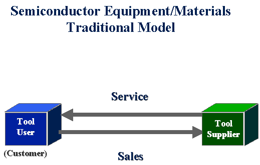
Focusing on the first decade in the new millenium, the Convergence Era, a further change in the relationship between the manufacturer (tool user) and the vendor (tool or material supplier) becomes evident. Prior to the concept of Global Account Management, the Traditional Model could be represented as follows:
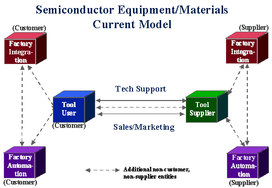
Today, many large semiconductor manufacturers insist on having a dedicated support group provided by suppliers. The concept of Global Account Management (Integrators) has evolved from this need. With the increasing complexity of Factory Integration (FI)** and Factory Automation(FA)** requirements, a team approach with a vendor-supplied integrator will be the model for the next decade.
These Integrators will have to be sensitive to third parties which provide software to accommodate FI and third parties which provide robots, etc. for FA. These third parties will have an impact on the sale, installation, start up and eventual management of manufacturing tools. Additionally these third parties will be beholding to the tool user or the tool supplier but not both. A clear definition will have to be made as to which of the three or more parties involved will have responsibility for each part of the overall program. Communication between all the parties involved is the key to success. This communication will be the role of the Integrator. To quote Ken Levy, CEO of KLA, ". . . look for the integrators. They are the companies that semiconductor manufacturers will turn to and say 'Help me build these fabrication plants of the future. I want you to be my partner in this project.' Those kinds of companies will be winners…"
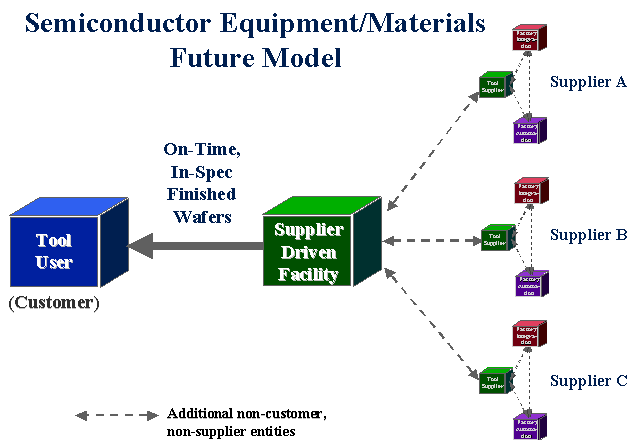
Global Account Management may change again towards the end of the next decade. Potentially semiconductor manufacturers could ask suppliers to provide the tools, processes, and personnel to run and maintain the plants and the materials to be processed. Initially this could be on a fixed fee basis but could evolve in a price per wafer processed. The groundwork for this can be found in the Cost of Ownership and Cost of Consumables models now in use. At that juncture, the role of the Integrator and its team will be even more critical to providing finished product in the form of processed wafers, in-spec and on-time.
The second decade of the new millenium will see the see the industry reinvent itself with such technologies such as organosilicides which will emulate how the brain works. The relationship between the parties will return to one of Scientist to Scientist. And so the process begins again.
*Special thanks to Dr. Robert Bratter for his input into this concept.
**Factory Integration (FI) is defined as control of the production process and tools by a host computer including interfab and intrafab communications. Factory Automation (FA) is defined as control of wafers and materials both interfab and intrafab. The complexity of these issues are extended by the fact that most of the fabs are custom in their design requirements and the suppliers have yet a different set of ideas.About the author
Bob Hills’ background includes sales, marketing and product management in the disciplines of etch, ion implantation, photolithography, spin-bake, PVD, CVD and semiconductor materials. He has held positions at Lam Research, Drytek/General Signal, Kasper Instruments/Eaton and Materials Research Corporation. He has a BSME and an MS in Metallurgy from Stevens Institute of Technology.
He can be reached at:523 Sunset Way, Redwood City, CA 94062 Phone:650-369-6993 E-mail:[email protected] www.questteam.com copyright © 1999 – 2025 all rights reserved (c)